


Introduction to SAR ADCs
Basic Concept and Overview
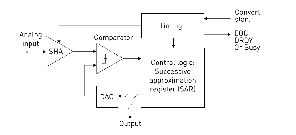
Figure 3: SAR architecture
Successive Approximation Register (SAR) Analog-to-Digital Converters (ADCs) hold a prominent position as a widely employed ADC variant, notably suited for applications necessitating a harmonious blend of conversion speed, power efficiency, and resolution. The operational foundation of the SAR ADC rests upon the utilization of a binary search algorithm, instrumental in guiding the ADC toward a convergent approximation of the input analog voltage. The term "successive approximation" refers to the iterative method used by the ADC to estimate the analog input voltage. It works by gradually refining its approximation over steps, getting closer to the actual input voltage each time.
The Successive Approximation Register is the central component of the SAR ADC. Within this register, the binary value stands as a representation of the present approximation of the input voltage. In each step of the conversion process, the SAR control logic systematically adjusts a single bit of this approximation, commencing from the most significant bit (MSB) and advancing down to the least significant bit (LSB).
An indispensable constituent of the SAR ADC configuration is the Digital-to-Analog Converter (DAC). Functioning in harmony with the SAR control logic is the DAC which undertakes the task of translating the ongoing approximation stored in the SAR register into an analog voltage. Subsequently, this analog voltage is matched against the input voltage. Should the DAC's output fall short of the input voltage, the particular bit being scrutinized maintains its set state; in contrast, if it surpasses the input voltage, the bit is reset. This iterative procedure continues its course, traversing down the progression until reaching the least significant bit (LSB).
In the operational sequence of a typical SAR ADC, the following steps are undertaken:
- The input analog voltage is acquired an held at a constant value.
- Initialization begins with setting the Most Significant Bit (MSB) of the SAR register, prompting the DAC to produce the corresponding analog voltage output.
- The comparator evaluates the DAC output against the input voltage, and this outcome influences the SAR register through an update process.
- After the comparison, the next bit within the SAR register is subjected to testing, perpetuating the cycle until the Least Significant Bit (LSB) has undergone examination.
- Upon completion of the testing iterations, the ultimate value present in the SAR register signifies the digital representation of the input analog voltage.
The SAR ADC distinguishes itself with its efficient functionality at moderate speeds. In contrast to Flash ADCs, which necessitate numerous comparators to attain heightened resolution, the SAR ADC relies on a solitary comparator and accomplishes resolution progressively through iterative approximations. This distinctive characteristic renders the SAR ADC notably efficient concerning power consumption and component count, particularly within the domain of moderate to high resolutions.
Architecture of SAR ADCs
Sample and Hold Circuit
The Sample and Hold Circuit constitutes a foundational component within the SAR ADC's framework. It operates as the initial point of entry for the analog signal into the ADC system. Fundamentally, the Sample and Hold Circuit executes the dual task of sampling the incoming analog voltage and subsequently maintaining it at a consistent level throughout the conversion process. This circuit's significance emerges from the potential temporal variability of the analog signal, necessitating a stabilized voltage level for accurate ADC conversion.
Comparator
The Comparator stands as another pivotal facet inherent to the SAR architecture. Following the collection and stabilization of the analog input voltage by the Sample and Hold Circuit, the Comparator takes on the responsibility of evaluating this held voltage. In doing so, it undertakes a comparison against a reference voltage produced by the internal Digital-to-Analog Converter (DAC). Through this comparison, the Comparator produces a binary output, signifying whether the sampled input voltage exceeds or falls short of the reference voltage. The outcome of this comparison assumes a critical role in guiding the operations of the Successive Approximation Register, influencing the iterative refinement of the ADC's approximation of the input voltage.
Digital-to-Analog Converter (DAC)
The Digital-to-Analog Converter employed within the SAR ADC assumes a distinctive role. In contrast to stand-alone DACs, which primarily transform digital signals like audio into analog form, the DAC integrated into a SAR ADC undertakes an internal function which is to generate reference voltages. These reference voltages are subsequently pitted against the sampled input voltage for comparison. Driven by the prevailing binary pattern stored in the Successive Approximation Register, the DAC's operation contributes to the iterative process of approximation. As the SAR progressively hones its estimation, the DAC adapts to produce increasingly precise reference voltages.
Successive Approximation Register
At the core of the SAR ADC resides the pivotal Successive Approximation Register (SAR). This component serves as the very essence of the SAR ADC's operation, embodying the essence of the successive approximation algorithm. The SAR commences its operation with an initial approximation and subsequently advances its refinement through a sequence of successive comparisons. In the case of an n-bit ADC, this equates to n individual comparisons, commencing from the Most Significant Bit (MSB) and concluding at the Least Significant Bit (LSB). Post each comparison, the SAR modifies the bit currently under scrutiny. If the output from the DAC registers a value lower than the input voltage, the bit being examined is set to 1; conversely, it is set to 0. This iterative process persists until the entirety of the conversion procedure is concluded.
Operation of SAR ADCs
Binary Search Algorithm
The fundamental operational principle of SAR (Successive Approximation Register) ADCs hinges upon the binary search algorithm, an iterative technique employed to progressively narrow down the feasible range within which the analog input value resides. This algorithm functions by scrutinizing each bit, commencing from the most significant bit (MSB) and concluding at the least significant bit (LSB), to discern the closest match to the actual analog input.
The initiation of the binary search involves setting the MSB to 1 while keeping all other bits at 0. Subsequently, this binary pattern is converted into an analog reference voltage using the DAC. This resultant reference voltage is then juxtaposed against the sampled input voltage. If the comparison reveals that the reference voltage is lower than the input voltage, the MSB retains its set value of 1; conversely, if the reference voltage surpasses the input voltage, the MSB is set to zero. This process iteratively recurs for the subsequent bits, merging the outcomes of preceding bit assessments with the one currently under examination, until the entire bit sequence has undergone evaluation. For instance, in a scenario involving a 3-bit ADC. The initial approximation could be 100 (in binary), equivalent to a decimal value of 4. Should this initial approximation prove to be insufficient, the subsequent approximation might evolve to 110 (in binary), corresponding to a decimal value of 6, and so forth, until the ultimate approximation is ascertained.
Conversion Cycle
The SAR ADC conversion cycle encapsulates the process of transforming an analog input into a corresponding digital output. The cycle unfolds with the initiation of sampling, during which the input voltage is captured and stabilized by the Sample and Hold Circuit. Following this phase, the binary search algorithm is set into motion to approximate the digital rendition of the sampled voltage. Each iteration of the binary search aligns with a single clock cycle, thus correlating to the ADC's clocking mechanism. In the context of an n-bit ADC, the cycle comprises n clock cycles, precisely one for each bit being processed.
Upon the culmination of these n cycles, the digital output materializes within the SAR, becoming accessible for retrieval. After this, the ADC is primed to initiate a fresh conversion cycle, thereby perpetuating its operational sequence.
It merits attention that the temporal duration required to execute a conversion is directly linked to the ADC's resolution, which corresponds to the number of bits utilized. Consequently, under a consistent clock rate, an augmentation in resolution engenders a corresponding elevation in conversion time. This interplay between resolution and speed necessitates thoughtful consideration when orchestrating systems that incorporate SAR ADCs, as it underscores an essential trade-off to be weighed during the design phase.
Advantages of SAR ADCs
Efficiency at Moderate Speeds
SAR ADCs have garnered considerable acclaim for their adeptness in efficiently transmuting analog signals into digital form, particularly when operating at moderate speeds. This efficiency is chiefly attributed to their employment of the binary search algorithm, a feature that expedites the precision of the analog value through the iterative assessment of each bit. This method stands in stark contrast to algorithms that necessitate the evaluation of every feasible value, a characteristic often observed in integrating ADCs.
In a multitude of applications ranging from sensor data acquisition to audio processing, there is often no pressing requirement for ultra-high-speed conversions. In such contexts, the SAR ADC emerges as an exemplary solution, aptly striking a harmonious equilibrium between the pace of conversion and the inherent intricacy of the process. This attribute proves particularly advantageous when juxtaposed with algorithms utilized in delta-sigma ADCs or flash ADCs, which tend to be swifter or slower, respectively. The SAR ADC's intermediate speed profile renders it a suitable candidate for an array of scenarios where the emphasis lies on efficient data throughput, without neglecting essential considerations such as power consumption and component cost.
Low Power Consumption
One of the foremost advantages of SAR ADCs lies in their remarkable power efficiency. In contrast to Flash ADCs, which necessitate the operation of numerous comparators in parallel, SAR ADCs harness the prowess of a solitary comparator, making decisions in a step-by-step manner, bit by bit. This design characteristic engenders a substantial reduction in the ADC's power consumption, especially during periods of inactivity.
The capacity of SAR ADCs to conduct conversions with fewer transistors and diminished capacitance compared to parallel architectures, such as Flash ADCs, assumes pivotal importance in curtailing power consumption. This attribute becomes particularly advantageous in applications reliant on battery power, where optimizing energy efficiency stands as a critical priority.
Moreover, select SAR ADCs offer power-down modes, a feature that serves to further diminish power consumption during instances when the ADC is not actively engaged in conversion processes. This capability bears particular relevance in contexts like sensor nodes, where periodic measurements are requisite and judicious power management between measurements holds paramount importance.
Disadvantages of SAR ADCs
While Successive Approximation Register (SAR) ADCs provide significant advantages, it is critical to understand their limitations and downsides to make informed design decisions. This section will go through the major drawbacks of SAR ADCs.
Resolution Limitations: The resolution capabilities of SAR ADCs are fundamentally limited. While they perform effectively for jobs requiring intermediate resolution, they fall short when faced with high-resolution needs. Essentially, as the resolution requirement grows, the inherent design limits of SAR ADCs become more obvious.
Slower Conversion Speeds at High Resolutions: A fundamental attribute of SAR ADCs is that with the escalation of the resolution, a proportional increase in the requisite number of bits for precise approximation unfolds, consequently necessitating a greater number of conversion steps. This augmented step count consequently engenders a deceleration in the conversion process. Hence, while SAR ADCs adeptly manage moderate speeds efficiently at lower resolutions, their operational pace experiences a decline as the need for higher resolution arises.
Sensitivity to Clock Jitter: Clock jitter holds a pronounced influence over the performance of a SAR ADC, given its reliance on the clock signal to orchestrate the successive approximation stages. Minute deviations in the timing of the clock signal can also introduce inaccuracies, a concern particularly relevant at elevated sampling rates. This susceptibility to clock jitter carries the potential to curtail the effective resolution and dynamic performance of SAR ADCs, especially within the domain of high-frequency applications.
Linearity Errors: Ensuring accurate representation of an analog signal hinges on maintaining linearity. In SAR ADCs, linearity is intrinsically linked to the performance of the internal Digital-to-Analog Converter (DAC). Any degree of non-linearity present in the DAC has the potential to introduce errors during the conversion process. While employing high-performance DACs can alleviate this concern, it often results in an elevation of both cost and intricacy within the ADC system.
Noise Susceptibility: SAR ADCs display a heightened vulnerability to noise when juxtaposed with other ADC types like delta-sigma ADCs. This susceptibility is largely attributable to the absence of oversampling and noise shaping techniques, which are commonly employed in noise reduction strategies. Consequently, SAR ADCs might not be the optimal choice for scenarios wherein noise performance is of paramount importance.
Glitch Impulse: Within the binary search algorithm's DAC settling period, there exists the possibility of transient voltage spikes known as glitches. These glitches, when they occur, can inadvertently introduce errors into the ADC conversion process, particularly in high-frequency applications where rapid changes are prevalent. This phenomenon underscores the importance of addressing glitch-related challenges, especially when utilizing SAR ADCs in contexts characterized by elevated frequencies.
Applications Suited for SAR ADCs
Successive Approximation Register (SAR) ADCs find use in a variety of applications because of their low power consumption and moderate speed. This section describes two key applications for SAR ADCs: data logging and sensor interfaces.
Data Logging
One of the notable applications wherein SAR ADCs find prominence is in the realm of data logging. Data logging entails the accumulation of data across time intervals, frequently adhering to a consistent sampling rate. This data compilation encompasses a diverse array of parameters, encompassing environmental facets such as temperature, humidity, or pressure, as well as system-related variables such as voltage, current, or power consumption.
In the context of data logging, SAR ADCs offer an advantageous fit for several reasons:
Power Efficiency: Data logging applications mostly mandate sustained operation for extended durations, occasionally reliant on battery power. The intrinsic characteristic of SAR ADCs, characterized by low power consumption, positions them optimally for these specific scenarios.
Moderate Speed: Data logging operations typically do not necessitate rapid conversion speeds. The moderate pace exhibited by SAR ADCs often proves to be abundantly suitable for the demands of data logging applications. The ability of SAR ADCs to function effectively within this moderate speed spectrum aligns well with the temporal requisites of data logging.
Flexibility in Resolution: SAR ADCs extend a valuable attribute of adaptability with respect to resolution, allowing for the selection of resolutions tailored to the unique requirements of specific applications. In the domain of data logging, where a moderate level of resolution is commonly sought, SAR ADCs excel in efficiently delivering the necessary precision.
Sensor Interfaces
SAR ADCs find extensive utility in sensor interfaces, constituting yet another pivotal domain of application. Sensors are instrumental in measuring diverse physical quantities and subsequently translating them into discernible signals interpretable by instruments or processors. A broad spectrum of sensors, including temperature sensors, pressure sensors, accelerometers, and light sensors, can seamlessly interface with SAR ADCs to facilitate accurate and precise data conversion.
The reasons for the suitability of SAR ADCs for sensor interfaces include:
Precision: The precision demanded by many sensors necessitates accurate analog-to-digital conversion. Notably, SAR ADCs possess the capacity to deliver the requisite precision without entailing undue power consumption.
Fast Settling Time: The concept of settling time in SAR ADCs pertains to the duration taken for the converter to establish a stable output after an alteration in the input signal. A swifter settling time corresponds to a more rapid ADC responsiveness to fluctuations in the sensor output. SAR ADCs, recognized for their notably expedient settling times, prove invaluable in contexts demanding prompt adaptation to swift variations in sensor signals.
Low Latency: In the realm of control systems, minimizing latency between sensor readings and the system's ensuing response holds pivotal significance. The inherent capability of SAR ADCs to swiftly furnish a digital output proves immensely advantageous in scenarios that hinge on minimizing latency, ensuring swift and accurate system reactions.
Integration: SAR ADCs offer a compact form factor and notable integration capabilities, a facet that augments their utility within sensor interfaces. This attribute assumes heightened importance when devising compact or portable devices, as SAR ADCs contribute to the overall streamlined design and integration of the system.
Design Considerations and Trade-offs
When formulating a system that integrates a Successive Approximation Register (SAR) ADC, it becomes crucial to assess diverse factors to strike an ideal equilibrium among performance, expenses, and energy usage. This segment delves into the fundamental aspects to contemplate and the compromises to navigate when employing SAR ADCs.
Resolution and Conversion Speed: A pivotal compromise emerges between resolution and the pace of conversion. Generally, as the resolution of an ADC escalates, the time for conversion also elongates, attributable to the heightened number of clock cycles necessary to attain elevated precision. Selecting an appropriate resolution that aligns with the application's requisites while preserving a reasonable conversion speed remains a pivotal consideration.
Power Consumption and Performance: Despite SAR ADCs being renowned for their reduced power consumption in comparison to alternative ADC architectures, augmenting resolution and conversion rates may also result in heightened power usage. It is of paramount importance to meticulously scrutinize the power allocation within the application and assess the requisites for operational performance. This entails selecting an ADC configuration that adeptly navigates the delicate equilibrium between power conservation and optimal performance.
Input Impedance Matching: The presence of the Sample and Hold circuit within the SAR ADC can potentially introduce a capacitive load to the originating signal source. Such an occurrence can potentially yield detrimental effects, particularly in the case of high-impedance sources. Thus, due diligence is imperative in executing impedance matching protocols to guarantee the unfaltering accuracy of the ADC's signal sampling.
Reference Voltage Stability: The precision and stability of the reference voltage wield a profound influence over the accuracy of SAR ADC conversions. The consistent and dependable nature of the reference voltage source assumes pivotal significance, particularly in applications that place a premium on attaining remarkable accuracy levels. Effective measures must be implemented to ascertain the reference voltage's stability and minimal noise, thereby nurturing environments conducive to high-precision operations.
Noise Considerations: The presence of noise can significantly impact the accuracy of analog-to-digital conversion within the ADC. Opting for a suitable SAR ADC equipped with noise specifications that align with the application's requirements, coupled with the implementation of noise mitigation techniques such as filtering and signal averaging, assumes the utmost importance to ensure faithful signal digitization.
Cost and Complexity: The expense associated with a SAR ADC can exhibit substantial variation contingent on the desired resolution, speed, and incorporated features. Furthermore, the intricacies entailed in integrating a high-resolution SAR ADC could potentially entail additional components or sophisticated layout strategies. Accordingly, a prudent assessment of cost and complexity within the overarching framework of the project's budget and objectives is imperative.
ADC Driver Circuitry: The meticulous selection of ADC driver circuitry, encompassing operational amplifiers and anti-aliasing filters, stands as a linchpin to the SAR ADC's performance. The chosen driver circuit must furnish adequate bandwidth, minimal noise, and negligible distortion, meticulously aligned with the intended application's requisites, thus underpinning the overall efficacy of the SAR ADC's operation.
Log in to your account
Create New Account